Analytical expressions for the low-field mobility of the two dimensional electrons in mono layer graphene are obtained on base of quantum kinetic approach that is based on the one-particle density matrix and the model non-equilibrium distribution function in form of the shifted Fermi distribution. We consider the gated graphene with the Fermi level that is biased by applying an external voltage to the gate. In this case, the confining potential has the shape of a triangle well that can be written in terms of Airy functions. Screened acoustic, optic phonons and ionized impurities are considered as scattering mechanisms. Calculations show that in the semiconductors with Dirac spectrum of charge carriers mobility for scattering by acoustic phonons and ionized impurities does not depend on the electron effective mass. Both effective mass of electrons and scattering rate by non-polar optic phonons reach minimum for electron energy close to the Dirac point. A comparison of the temperature dependences of the calculated and experimental mobility data shows that in the temperature range under consideration, at T < 400 K mobility is determined by the scattering of electrons by ionized impurities. The acoustic and out-of-plane optical phonons (ZO phonons) determine the electron mobility at higher temperatures. Results of mobility calculations are compared with known experimental data.
| Published in | American Journal of Modern Physics (Volume 14, Issue 4) |
| DOI | 10.11648/j.ajmp.20251404.14 |
| Page(s) | 200-208 |
| Creative Commons |
This is an Open Access article, distributed under the terms of the Creative Commons Attribution 4.0 International License (http://creativecommons.org/licenses/by/4.0/), which permits unrestricted use, distribution and reproduction in any medium or format, provided the original work is properly cited. |
| Copyright |
Copyright © The Author(s), 2025. Published by Science Publishing Group |
Mobility, Mono Layer Graphene, Acoustic, Out-of-plane Optic Phonons, Ionized Impurities
 at room temperature offer significant advantages for applications ranging from fast electronics to touch screens and ultrasensitive photon detection
 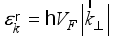 ,(1)
,(1)  m/sec is the Fermi velocity,
  is the wave vector,
  is the reduced Plank constant.
 ,(2)
,(2)  is the direction of quantum confinement.
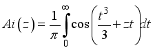
 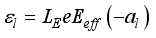 ,(3)
,(3) 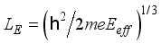 is characteristic length, Eeff is an effective surface field,
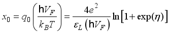
  is the electron charge,
  are zeros of the Airy functions that can be approximately given as
 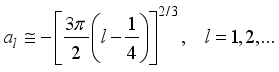 (4)
(4)  is the quantum number.
  the effective mass of electrons near the Dirac point can be written as
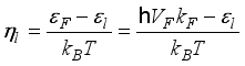
 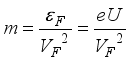 ,(5)
,(5) 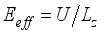 and expression for
  takes a form
 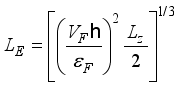 (6)
(6)  is the monolayer graphene thickness.
  can be obtained by integration
 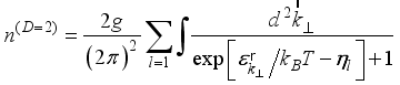 (7)
(7)  (8)
(8)  is the valley degeneracy, for graphene
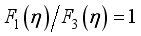
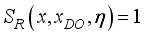
  .
.  .(9)
.(9)  are the Fermi-Dirac integrals
  (10)
(10) 
 (11)
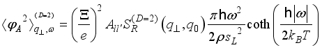
(11)  is the inverse mobility tensor
  . For isotropic effective mass the kinetic tensor
  degenerates into a scalar form. In the low-field limit the inverse mobility of carriers with dimensionality
  has the following form
  (12)
(12)  is the Fermi equilibrium distribution function,
  is the Boltzmann’s constant,
  is temperature,
  is the spectral correlator of scattering potential.
  into the final state
  , thus
  is the transferred momentum,
  is the change in energy at collision. The upper sign in argument of the Dirac delta function in (12) is used for phonon emission and the lower sing is used for phonon absorption.
  is the Heaviside step function that ensures a positive kinetic energy of electrons for scattering with emission of phonons (primarily for non-polar optic phonons). The scattering by acoustic phonons and ionized impurities we will consider as elastic (
  ).
).  by the inverse Fourier transform. The correlators for 3DEG scattering on by acoustic and non-polar optic phonons
 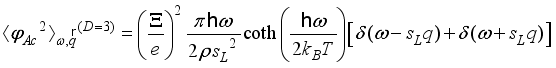 ,(13)
,(13) 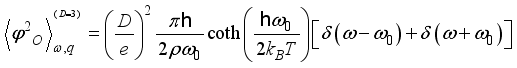 , (14)
  and
and  are the deformation potential coupling constants,
  is energy of non-polar optic phonon,
  and
and  are density of the crystal and velocity of the longitudinal acoustic phonon, respectively. Acoustic phonon scattering is treated within the elastic deformation potential approach in the long-wavelength acoustic-phonon limit.
  as follows:
 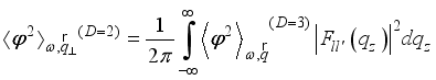 .(15)
.(15)  and
and  are the wave vectors for 2DEG and 3DEG, respectively.
  as follows:
  .(16)
.(16)  and
and  are the envelope functions in the confined direction
  ,(17)
,(17)  (18)
(18)  (19)
(19)  ,(20)
,(20)  (21)
(21)  (22)
(22)  is the screening factor and
  ,
,  ,
,  ,
,  .
.  , (23)
  is the inverse characteristic screening length.
 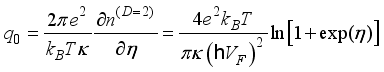 . (24)
  is the dielectric permittivity,
  and
and  are the vacuum and relative background dielectric constants, respectively.
 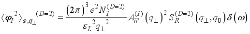 ,(25)
,(25)  is areal density of scattering centres.
 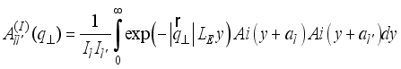 (26)
(26)  the overlap integral takes a form
 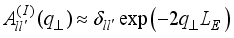 . (27)
 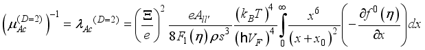 (28)
(28)  .(29)
.(29)  expression for mobility can be written as
 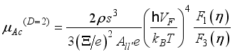 .(30)
.(30) 
 . (31)
 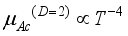 without screening effects. This dependence was obtained earlier
  expression for mobility simplifies
 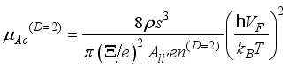 . (32)
 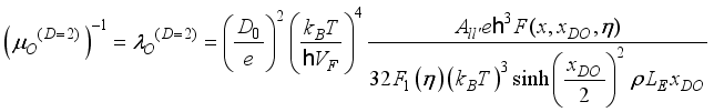 ,(33)
,(33) 
 .(34)
.(34) 
 ,(35)
,(35)  is the normalized energy of the non-polar optic phonons.
  ,
,  and expression (34) is significantly simplified.
 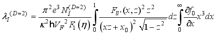 .(36)
.(36) 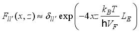 .(37)
.(37) 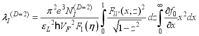 .(38)
.(38)  , non-polar optic
  phonons and ionized impurities
 (39)
(39)  (8) given by
  . (40)
  m/sec
m/sec 
 g/cm3
g/cm3 
 . The coupling constants for scattering by acoustic
  and Non-Polar optic phonons energy
  are considered as fitting parameters.
  used in calculations are in the range obtained previously
  is striking. This increase is due to the peculiarity of electron scattering on non-polar optic phonons. As it follows from (33) mobility for non-polar optic phonon scattering is proportional to
  which decreases with electron energy close to Dirac point where the electron effective mass
| [1] | J. H. Gosling. O. Makarovsky, F. Wang, et al. Commun Phys 4 30(2021). |
| [2] | W. Zhu, V. Perebeinos, M. Freitag, and P. Avouris Phys. Rev. B 80 235402 (2009). |
| [3] | I. I. Boiko Semiconductor Physics, Quantum Electronics & Optoelectronics 15 129(2012). |
| [4] | K. V. Nguyen and Y. Chang Phys. Chem. Chem. Phys. 22 3999 (2020). |
| [5] | S. H. Mir, V. K. Yadav and J. K.. Singh. ACS Omega 5 14203 (2020). |
| [6] | S. Das Sarma, S. Adam, E. H Hwang, and E. Rossi Rev. Mod. Phys. 83 407(2011). |
| [7] | E. H. Hwang, S. Das Sarma Phys. Rev. B 77 115449 (2008). |
| [8] | A. H. Castro Neto, F. Guinea, N. M. R Peres, K. S. Novoselov, and. A. K. Geim Rev. Mod. Phys. 81 109(2009). |
| [9] | D. Smith and L. von Smekal Phys. Rev. B 89 195429 (2014). |
| [10] | A. Majorana, G. Mascali, and V. Romano Journal of Mathematics in Industry 7 4(2017). |
| [11] | A. Akturka, and N. Goldsman J. Appl. Phys. 103 053702 (2008). |
| [12] | H. Hirai, H. Tsuchiya, Y. Kamakura, N. Mori, and M. Ogawa Journal of Applied Physics 116 083703 (2014). |
| [13] | T. Grasser, H. Kosina, S. Selberherr. In: Wachutka, G., Schrag, G. (eds) Simulation of Semiconductor Processes and Devices 2004. Springer, Vienna. |
| [14] | V. Chiloyan, S. Huberman, Z. Ding, J. Mendoza, A. A. Maznev, K. A. Nelson, and G. Chen Phys. Rev. B 104 245424 (2021). |
| [15] | G. Wilk, Z. Włodarczyk. Eur. Phys. J. A 57 221(2021). |
| [16] | B K Readly Quantum Processes in Semiconductors (Oxford University Press 2013). |
| [17] | R. S. Shishir, F. Chen, J. Xia, N. J. Tao, D. K. Ferry J Comput Electron 8 43(2009). |
| [18] | D. K. Ferry, S. M. Goodnick, and J. Bird Transport in Nanostructures. Cambridge University Press, Cambridge (2009). |
| [19] | I. I. Boiko Kinetics of Electron Gas Interacting with Fluctuating Potential. (Naukova dumka, Kiev, 1993). |
| [20] | K. L Kovalenko, S. I. Kozlovskiy, N. N. Sharan, E. F. Venger J. Phys.: Condens. Matter 36 325705 (2024). |
| [21] | K. L Kovalenko, S. I, Kozlovskiy, and N. N. Sharan AIP Advances 15 035156 (2025). |
| [22] | K. L Kovalenko, S. I Kozlovskiy, and N. N. Sharan J Comput Electron 17 926(2018). |
| [23] | X. Cong, Q. Q. Li, X. Zhang, M.-L. Lin, J. B. Wu, X. L. Liu, P. Venezuela, P. H. Tan Carbon 149, 19-24 (2019). |
| [24] | C. J. Shearer, A. D. Slattery J Stapleton Andrew, Shapter and Gibson C. T. Nanotechnology 27 125704 (2016). |
| [25] | S. V Morozov., K. S Novoselov, M. I Katsnelson, F. Schedin, D. C. Elias., J. A Jaszczak., and A. K.. Geim Phys. Rev. Lett. 100 01660 (2008). |
| [26] | Chen J. H., Jang C., Xiao S., Ishigami M. and Fuhrer M. S. Nature Nanotech 3 206(2008). |
| [27] | Tiras E., Ardali S., Tiras T., Arslan E., Cakmakyapan S., Kazar O., Hassan J., Janzen E., and Ozbay E. J. Appl. Phys. 113 04370 (2013). |
| [28] | R. S. Shishir and D. K. Ferry J. Phys.: Condens. Matter 21 232204 (2009). |
| [29] | D. L. Nika, E. P., Pokatilov and A. A. Balandin Phys. Status Solidi B 248 2609 (2011). |
| [30] | A Politano, F de Juan, G Chiarello, and H Fertig Physical Review Letters 115 075504 (2015). |
| [31] | A. A. Taleb, D. J. Farías Phys.: Condens. Matter 28 103005 (2016). |
| [32] | B. Hellsing, T, Frederiksen Phys. Rev. B 110 155426 (2024). |
APA Style
Kovalenko, K. L., Kozlovskiy, S. I., Sharan, N. N. (2025). Electron Mobility in Single-layer Graphene. American Journal of Modern Physics, 14(4), 200-208. https://doi.org/10.11648/j.ajmp.20251404.14
ACS Style
Kovalenko, K. L.; Kozlovskiy, S. I.; Sharan, N. N. Electron Mobility in Single-layer Graphene. Am. J. Mod. Phys. 2025, 14(4), 200-208. doi: 10.11648/j.ajmp.20251404.14
@article{10.11648/j.ajmp.20251404.14,
  author = {Konstantin Leonidovich Kovalenko and Sergei Ivanovich Kozlovskiy and Nicolai Nicolaevich Sharan},
  title = {Electron Mobility in Single-layer Graphene
},
  journal = {American Journal of Modern Physics},
  volume = {14},
  number = {4},
  pages = {200-208},
  doi = {10.11648/j.ajmp.20251404.14},
  url = {https://doi.org/10.11648/j.ajmp.20251404.14},
  eprint = {https://article.sciencepublishinggroup.com/pdf/10.11648.j.ajmp.20251404.14},
  abstract = {Analytical expressions for the low-field mobility of the two dimensional electrons in mono layer graphene are obtained on base of quantum kinetic approach that is based on the one-particle density matrix and the model non-equilibrium distribution function in form of the shifted Fermi distribution. We consider the gated graphene with the Fermi level that is biased by applying an external voltage to the gate. In this case, the confining potential has the shape of a triangle well that can be written in terms of Airy functions. Screened acoustic, optic phonons and ionized impurities are considered as scattering mechanisms. Calculations show that in the semiconductors with Dirac spectrum of charge carriers mobility for scattering by acoustic phonons and ionized impurities does not depend on the electron effective mass. Both effective mass of electrons and scattering rate by non-polar optic phonons reach minimum for electron energy close to the Dirac point. A comparison of the temperature dependences of the calculated and experimental mobility data shows that in the temperature range under consideration, at T < 400 K mobility is determined by the scattering of electrons by ionized impurities. The acoustic and out-of-plane optical phonons (ZO phonons) determine the electron mobility at higher temperatures. Results of mobility calculations are compared with known experimental data.},
 year = {2025}
}
TY  - JOUR
T1  - Electron Mobility in Single-layer Graphene

AU  - Konstantin Leonidovich Kovalenko
AU  - Sergei Ivanovich Kozlovskiy
AU  - Nicolai Nicolaevich Sharan
Y1  - 2025/07/31
PY  - 2025
N1  - https://doi.org/10.11648/j.ajmp.20251404.14
DO  - 10.11648/j.ajmp.20251404.14
T2  - American Journal of Modern Physics
JF  - American Journal of Modern Physics
JO  - American Journal of Modern Physics
SP  - 200
EP  - 208
PB  - Science Publishing Group
SN  - 2326-8891
UR  - https://doi.org/10.11648/j.ajmp.20251404.14
AB  - Analytical expressions for the low-field mobility of the two dimensional electrons in mono layer graphene are obtained on base of quantum kinetic approach that is based on the one-particle density matrix and the model non-equilibrium distribution function in form of the shifted Fermi distribution. We consider the gated graphene with the Fermi level that is biased by applying an external voltage to the gate. In this case, the confining potential has the shape of a triangle well that can be written in terms of Airy functions. Screened acoustic, optic phonons and ionized impurities are considered as scattering mechanisms. Calculations show that in the semiconductors with Dirac spectrum of charge carriers mobility for scattering by acoustic phonons and ionized impurities does not depend on the electron effective mass. Both effective mass of electrons and scattering rate by non-polar optic phonons reach minimum for electron energy close to the Dirac point. A comparison of the temperature dependences of the calculated and experimental mobility data shows that in the temperature range under consideration, at T < 400 K mobility is determined by the scattering of electrons by ionized impurities. The acoustic and out-of-plane optical phonons (ZO phonons) determine the electron mobility at higher temperatures. Results of mobility calculations are compared with known experimental data.
VL  - 14
IS  - 4
ER  -
Department of Sensor Systems, V. Lashkaryov Institute of Semiconductor Physics, National Academy of Sciences of Ukraine, Kyiv, Ukraine
Department of Sensor Systems, V. Lashkaryov Institute of Semiconductor Physics, National Academy of Sciences of Ukraine, Kyiv, Ukraine
Department of Sensor Systems, V. Lashkaryov Institute of Semiconductor Physics, National Academy of Sciences of Ukraine, Kyiv, Ukraine
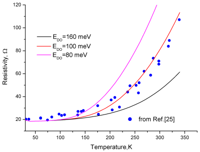
Figure 1. Experimental (circles) [25] and calculated (![]() ,
,![]() ) (solid lines) temperature dependences of resistivity single-layer graphene are shown for different values of optic phonon energies
) (solid lines) temperature dependences of resistivity single-layer graphene are shown for different values of optic phonon energies ![]() .
.
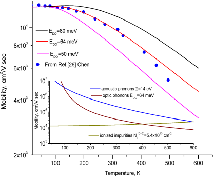
Figure 2. Experimental (circles) [26] and calculated (![]() ,
,![]() ) (solid lines) temperature dependences of mobility are shown for different values of the optic phonon energy
) (solid lines) temperature dependences of mobility are shown for different values of the optic phonon energy![]() . The inset shows the contribution of different scattering mechanisms to temperature dependence of electron mobility.
. The inset shows the contribution of different scattering mechanisms to temperature dependence of electron mobility.
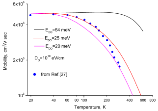
Figure 3. Experimental (circles) [27] and calculated (![]() ,
,![]() ) (solid lines) temperature dependences of mobility are shown for different energies of Non-Polar optic phonons
) (solid lines) temperature dependences of mobility are shown for different energies of Non-Polar optic phonons![]() .
.
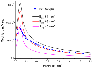
Figure 4. Experimental (circles) [28] and calculated (solid lines) dependences of mobility on electron density in single-layer graphene are shown at 300K for different values for different values of the optic phonon energy ![]() .
.
Information